He encontrado que alguna farmacia puede tener existencias limitadas de ciertos medicamentos, mientras que otras pueden tener casi cualquier formato que se le ocurra y el habitual de dosis habitualidad apareció. En resumen, siempre se contiene el almacén de corroborar. Al mismo tiempo que el producto que más que gustaba ha resultado no estaba disponible en stock otro distinto por las Buenas costumbres también debe buscarse jefe no asн parezca. Por eso es importante disponer de un Plan B para actuar cuandod ello no ocurra.
Ventaja de tomar un genérico en lugar de Asix
Un genérico es más barato que el nombre de marca
Uno de los mayores incentivos para someterse al Dónde comprar Lasix genérico en lugar de pagar la marca es que usted puede obtener un ahorrando importantes Lasix genérico. Por lo tanto, un Lasix genérico es en general mucho más barato que el homólogo de marca, así que una denominación genérica se hace posible para las personas que usan este medicamento con frecuencia. Un ejemplo: La compra de lurosemida en lugar de Lasix es una considerable ahorro para el presupuesto mensual de medicamentos.
Pmc fpga modules excel at image processing
30765 S Wixom Rd, PO Box 437, Wixom, MI 48393-7037 USA
Tel: 248-624-1541 Fax: 248-624-9234 www.acromag.com
Acromag PMC FPGA Boards Excel at Image Processing
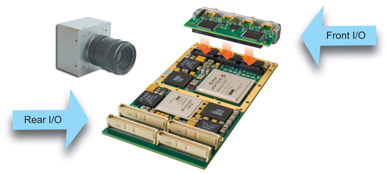
Over the past several months, Acromag has engaged in a number of image processing applications based upon implementations of Camera Link running on a Virtex-5 FPGA module. In several of these instances, LVDS signals are used to collect the image data through front and/or rear I/O connections on the PMC FPGA module. Other applications use a custom interface developed for selected imaging devices to capture data through the PMC module’s front and rear I/O interfaces. To select the appropriate FPGA module for image processing applications engineers must consider a number of pertinent criteria. Finding an appropriate Commercial-Off-The-Shelf (COTS) FPGA module for image processing depends on a number of key factors: I/O interface, frame speed, frame size, on-board processing requirements, and host communication speed/volume. The Xilinx Virtex-5 FPGA devices found on Acromag’s latest COTS PMC Modules offer blazing 550MHz processing speed and a variety of high-performance memory options that are well-suited to image processing functions. Table 1: Acromag PMC modules with re-configurable Virtex-5 FPGAs
Dual-Port Total Block DSP48E Capacity Capacity Number Cells RAM(Kbits) Slices
Note 1: Available increments are 32M, 64M, and 128M (contact factory) Note 2: Available increments are 256K, 512K, and 1024K (contact factory)
Acromag is an ISO 9001 and AS9100 certified manufacturer.
Video image capture is most frequently performed using direct access to the LVDS data lines available through Acromag’s AXM-D04 front mezzanine card or through the rear I/O P4 PMC connector. Alternatively, some applications use Camera Link interface chips on either a custom rear transition module or a custom AXM mezzanine module. The objective of these interfaces is to capture one whole raw image frame into storage on the PMC Module. There are three modes of Camera Link (base, medium, and full) which differ in the number of bits utilized in the raw image frame capture and provide for standardized hardware connections as defined in the Camera Link specification. Upon successful acquisition of a raw image frame, several processing objectives are possible: event detection, storage, enhancement/storage, or overlay/enhancement/storage. Figure 1: Event Detection
Event detection involves executing a predetermined algorithm on the raw image frame to determine the presence or absence of an event. The event could be the presence of an object, the absence of an object, the movement of an object (based upon comparison with prior frames), or a characteristic of an object (color, temperature, texture, size, etc.). For simple event detection, it will suffice to have just enough memory to accommodate the raw image frame and any comparison frame(s), sufficient logic cells for the event detection algorithm, and the I/O required for the event signaling mechanism. Figure 2: Storage
Storage involves moving the captured raw image frame to a location within the FPGA, on the PMC module, or to temporary FIFO storage for transfer to the system CPU via a mechanism such as DMA. Temporary storage may be accommodated on the PMC FPGA module. One must remember that the FPGA PMC memory is volatile. Any information destined to be of large volume and/or stored long-term will need to be FIFO buffered and moved to a permanent storage device such as a disk drive connected to the system CPU. The criteria for successful implementation of this objective involve ensuring that the rate of moving frames to permanent storage exceeds the rate of capture and buffering. Dual-port SRAM is important for FIFO buffering and DMA transfer. Standard modules support 256K x 64 bits and can be increased to either 512K x 64 bits or 1024 x 64 bits. Acromag’s Virtex-5 FPGA PMC modules support PCI-X with 32 or 64-bit wide transfers at bus frequencies up to 133MHz.
Acromag is an ISO 9001 and AS9100 certified manufacturer.
Raw image enhancement is a complicated process which increases the resolution of detectable events or criteria for actionable decision-making. It may involve removing noise, adjusting contrast, sharpening edges, softening, color correction, removing/adding baseline patterns or masks, and more – all in an effort to make event detection possible. There may even be multiple stages or outputs of the raw image enhancement process. As described above, one such process output is for actionable decision-making, yet another may be for visual review on a monitor. Once a raw image is enhanced, it would be stored locally in a FIFO and subsequently transferred to a more permanent storage. The enhancement/storage process increases the performance and memory requirements of the previously described storage objective. Processing of the raw image requires more FPGA logic cycles. The potential of generating more than one enhanced image necessitates increased FPGA PMC storage. Transfer of the now enhanced image(s) to the system CPU will conceptually require more DMA buffering and increase PCI-X bus traffic. Figure 4: Enhancement/overlay/storage
Building on the enhancement/storage process, several raw images are enhanced in many applications using specific techniques applicable to the image type (visual, IR, UV, radar, ultrasound, X-ray, etc.). Images may be subsequently overlaid on top of another to generate a composite image. Stated simply, in these instances more processing power, more local memory, and more image input and image storage throughput are required.
Acromag is an ISO 9001 and AS9100 certified manufacturer. Proper FPGA Module Selection for Image Processing
The complexities and performance requirements of image processing are assisted greatly through the use of high-powered Virtex-5 FPGA-based PMC modules. See Table 1. When large application logic segments are required, the champions will be the PMC-VLX155, PMC-VLX110 and the PMC-VSX95. These models feature the largest numbers of logic cells. When complex transforms and high computational throughput are required, the platforms of choice are the PMC-SX95, followed by the PMC-VLX155 and the PMC-VFX70. These models have a large number of DSP48e slices and a large logic cell count which can be used to encode complex dedicated algorithms. Sometimes, designing logic around a CPU core may prove beneficial. It may be useful for executing logic written in a higher level language (vs. VHDL). Additionally, an OS-based environment may be easier to implement or provide better data management capabilities. In these cases, the primary candidate would be the PMC-VFX70 with a hard core embedded PPC440. A PMC-VSX95 or PMC-VLX155, with their large quantity of logic cells, could also be used to accommodate the soft core processor of choice. The breadth of available Virtex-5 FPGA PMC modules from Acromag makes it possible to work with a family of products that have a similar “look and feel.” This flexibility makes it much easier to either increase performance or reduce the size and cost of the FPGA module as application requirements change. As a result, many engineers are now deploying Acromag PMC FPGA modules for their image processing applications. If you have questions, please contact us at Acromag. Rowland S. Demko Regional Sales Manager Acromag Incorporated 30765 S. Wixom Road Wixom, Michigan 48393-7037 USA Phone: 1-248-624-1541 Direct: 1-248-295-0825 Fax: 1-248-624-9234 Email: [email protected] WEB: WWW.Acromag.com
Acromag is an ISO 9001 and AS9100 certified manufacturer.
The Supreme Court Case of Marley v. Rawlings & Another: A Mix-Up in Wills In December 2013, the Supreme Court heard the ongoingdispute between two biological brothers and their‘adopted’ sibling af ter their parents, Alf red Rawlings andMaureen Rawlings, mistakenly signed each other’s wil s. The issues bef ore the Supreme Court were:(1) Whether, when a person mistakenly execut
Inca Trail and Machu Picchu August 2011 Trip Information Packet Hike the Inca Trail from Cuzco, Peru to Machu Picchu with Joel Malm. Joel will lead daily leadership devotionals on the trail. Your final day of hiking will end in Machu Picchu, one of the new 7 Wonders of the World. The theme of the hike will be Simplify . Dates: Schedule: Spend the day acclimatizing

 30765 S Wixom Rd, PO Box 437, Wixom, MI 48393-7037 USA
Tel: 248-624-1541 Fax: 248-624-9234 www.acromag.com
Acromag PMC FPGA Boards Excel at Image Processing
30765 S Wixom Rd, PO Box 437, Wixom, MI 48393-7037 USA
Tel: 248-624-1541 Fax: 248-624-9234 www.acromag.com
Acromag PMC FPGA Boards Excel at Image Processing