He encontrado que alguna farmacia puede tener existencias limitadas de ciertos medicamentos, mientras que otras pueden tener casi cualquier formato que se le ocurra y el habitual de dosis habitualidad apareció. En resumen, siempre se contiene el almacén de corroborar. Al mismo tiempo que el producto que más que gustaba ha resultado no estaba disponible en stock otro distinto por las Buenas costumbres también debe buscarse jefe no asн parezca. Por eso es importante disponer de un Plan B para actuar cuandod ello no ocurra.
Ventaja de tomar un genérico en lugar de Asix
Un genérico es más barato que el nombre de marca
Uno de los mayores incentivos para someterse al Dónde comprar Lasix genérico en lugar de pagar la marca es que usted puede obtener un ahorrando importantes Lasix genérico. Por lo tanto, un Lasix genérico es en general mucho más barato que el homólogo de marca, así que una denominación genérica se hace posible para las personas que usan este medicamento con frecuencia. Un ejemplo: La compra de lurosemida en lugar de Lasix es una considerable ahorro para el presupuesto mensual de medicamentos.
Da6011b_001.doc
MAS6011B Solar Cell Energy Harvesting System Manager
• Ultra Low Power, 110nA
• Low Battery Indicator
• Precise Power Up/Down
• Battery Overcharging Protection DESCRIPTION
The MAS6011 solar cell system manager monitors
protection of a secondary 3V battery over a big
the supply voltage and charging of a battery-
powered system containing a small solar cell. The
current consumption of this IC is extremely low, 110
Three output signals indicate the state of the
nA, which means the system can charge from very
system. Power Down (XPD) indicates whether the
low light conditions and also stay in power down
supply voltage is high enough to power up and run
mode for years and still operate directly from the
the system. Low Battery (LB) is used to signal the
condition when the battery capacity is low and
when to move to power saving mode. The third
To be able to charge a battery also in condition with
signal, SOL, is used for battery charging control.
very limited light, a large solar cell is usually used.
When the battery is full it bypasses the charging
This can on the other hand easily destroy the
current by an internal shunt switch to avoid
battery due to over voltage during strong sun light.
overcharging. The SW pin can also be used to
MAS6011 solves this dilemma and will give secure
control an external shunt switch for higher currents.
FEATURES APPLICATIONS
• Ultra Low Current Consumption, typ 110nA
• Low Supply Voltage Operation, min 2.0V
• Power On Indicator and secure Power ON after
• Deep discharge protection of battery during
• Precise Shut Down and precise Low Battery
• Suitable for rechargeable 3V Lithium Vanadium
FUNCTIONAL DESCRIPTION
The solar manager generates three main signals:
conductive but when the power supply voltage rises
XPD (Power Down), LB (Low Battery) and SOL
too much this switch is switched on to shunt the
(Solar Charging). The fourth SW signal is for
solar cell charging current and to prevent battery
controlling an optional external PMOS transistor.
capability of the internal PMOS switch is typically
These signals are produced by three comparators
28 mA. If a larger shunt current is needed an
which have hysteresis build in. Each comparator
external PMOS transistor can be used controlled by
compares the supply voltage (VDD) to the internal
switching levels. The current consumption of the
comparators is extremely low. The electrical
In operation without an external Schottky diode
parameters are described more detailed in the
between the pins SOL and GND, the voltage at pin
SOL is clamped to about 700 mV below GND by an
internal diode-connected NPN transistor.
The XPD signal can be used to power down the
whole system whenever the supply voltage level has dropped too low (see application figure 4).
MAS6011 does not have any control pin. After the
When the supply voltage is too low the XPD goes
power supply is connected the device is ready to be
low to power down the solar powered system.
When the supply voltage is high enough the XPD
goes high controlling power up condition.
The XPD, LB and SOL/SW switching levels have
been designed for usage with VL-type rechargeable
For a low power system (max current consumption
lithium vanadium pentoxide batteries. Those
1mA) the XPD pin output can be used as a system
batteries are compact, high energy secondary
supply voltage (see application figure 5) to keep the
batteries that have nearly twice the energy of
systems current consumption to a minimum.
conventional button-shaped Ni-Cd batteries. The
self discharge rate is less than 2% a year which
The LB signal indicates that the battery is low but
makes them very useful as a power source in
not empty. It can be used to control the system into
systems that might be stored for a long time without
a power saving mode. In power on (XPD=high) LB
goes high when supply voltage level is too low and LB goes low when supply voltage level is high
enough. In power down (XPD=low) the LB is low.
Figure 1 illustrates the MAS6011 functions and
shows the comparator switching levels for both
SOL is used for controlling the charging of the
battery charging (rising VDD) and discharging
rechargeable battery. Normally the internal PMOS
switch between VDD and the SOL pin is non-
FUNCTIONAL DESCRIPTION
SOL_OFF (charging off) SOL_ON (charging on) BATTERY CHARGING BATTERY DISCHARGING (VDD RISING) (VDD FALLING) LB_OFF (LB=low) XPD_OFF (XPD=high) (LB=high) XPD_ON (XPD=low) Figure 1. MAS6011 functions ABSOLUTE MAXIMUM RATINGS Parameter Symbol Conditions Min
Stresses beyond those listed may cause permanent damage to the device. The device may not operate under these conditions, but it will not be destroyed. This is a CMOS device and therefore it should be handled carefully to avoid any damage by electrostatic voltages (ESD). The most sensitive pin for the ESD is the SOL pin.
ELECTRICAL CHARACTERISTICS: MAS6011BA1 (3V BATTERY, MCU VDDmin ≤ 2.1V)
Operating Conditions: TA = -40°C to +85°C, typical values at TA = +27°C, unless otherwise specified.
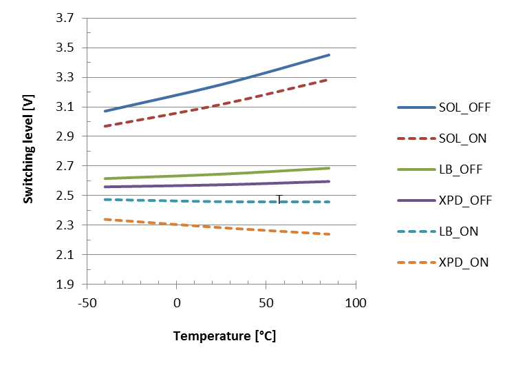
Parameter Symbol Conditions Min ELECTRICAL CHARACTERISTICS: MAS6011BA1 (3V BATTERY, MCU VDDmin ≤ 2.1V) [nA] 100 Temperature [°C] Figure 2. Typical temperature dependency of IDD Figure 3. Typical temperature dependency of comparator switching levels TYPICAL APPLICATION
Schottkydiode:VishaySD103Aor similar.
Figure 4. Typical application circuit of MAS6011BA1 – XPD for power down control of solar powered system
Schottkydiode:VishaySD103Aor similar.
Figure 5. Typical application circuit of MAS6011BA1 – XPD as supply voltage for a low power microcontroller TYPICAL APPLICATION
Figure 6. Typical application circuit of MAS6011BA1 – external PMOS transistor shunt for solar current Figure 7. Typical application – Wireless sensor system with Time Code Reception The system in figure 7 shows a wireless module that can receive both the AM long wave Time Code Signal as well as measuring different physical parameters via several sensors. The information is transmitted via a low power RF transmitter to a receiver indoors. By placing the module where the Time Code signal is strong good reception can be accomplished also in buildings normally blocking this signal. The low power consumption of the MAS6011 together with the energy harvesting solar cell enables this system to operate without the need for battery replacement. MAS6011BA1 IN QFN 3x3 PACKAGE QFN 3x3 6ld QFN 3x3 PIN DESCRIPTION
Function
NC = Not Connected, P = Power, G = Ground, DO = Digital Output, AO = Analog Output
PACKAGE (QFN 3X3x0.75 6ld) OUTLINE
SHAPE OF PIN #1 IDENTIFICATION IS OPTIONAL Symbol Min Nom Max Unit
Dimensions do not include mold or interlead flash, protrusions or gate burrs.
ORDERING INFORMATION
Product Code Product Package Comments LOCAL DISTRIBUTOR
MATERIAL SAFETY DATA SHEET Perigen® Defence Residual Insecticide Date of Issue: January 5th, 2004 1. IDENTIFICATION OF THE SUBSTANCE / MIXTURE AND SUPPLIER Product name: Perigen® Defence Residual Insecticide Other names: Product code: Recommended A liquid insecticide concentrate for use in general purpose pest control and Supplier: Bayer Environmental Scie
 ELECTRICAL CHARACTERISTICS: MAS6011BA1 (3V BATTERY, MCU VDDmin ≤ 2.1V)


 TYPICAL APPLICATION